
News detail
30 Days from Zero to Mass Production! Taixin Semiconductor × Claude Opus AI Redefines the Limits of IPC Mass Production Speed
How fast can a smart hardware device go from project initiation to mass production? The answer is <30 days. Recently, a limited-edition 1080P smart camera has sparked considerable…

How fast can a smart hardware device go from project initiation to mass production?
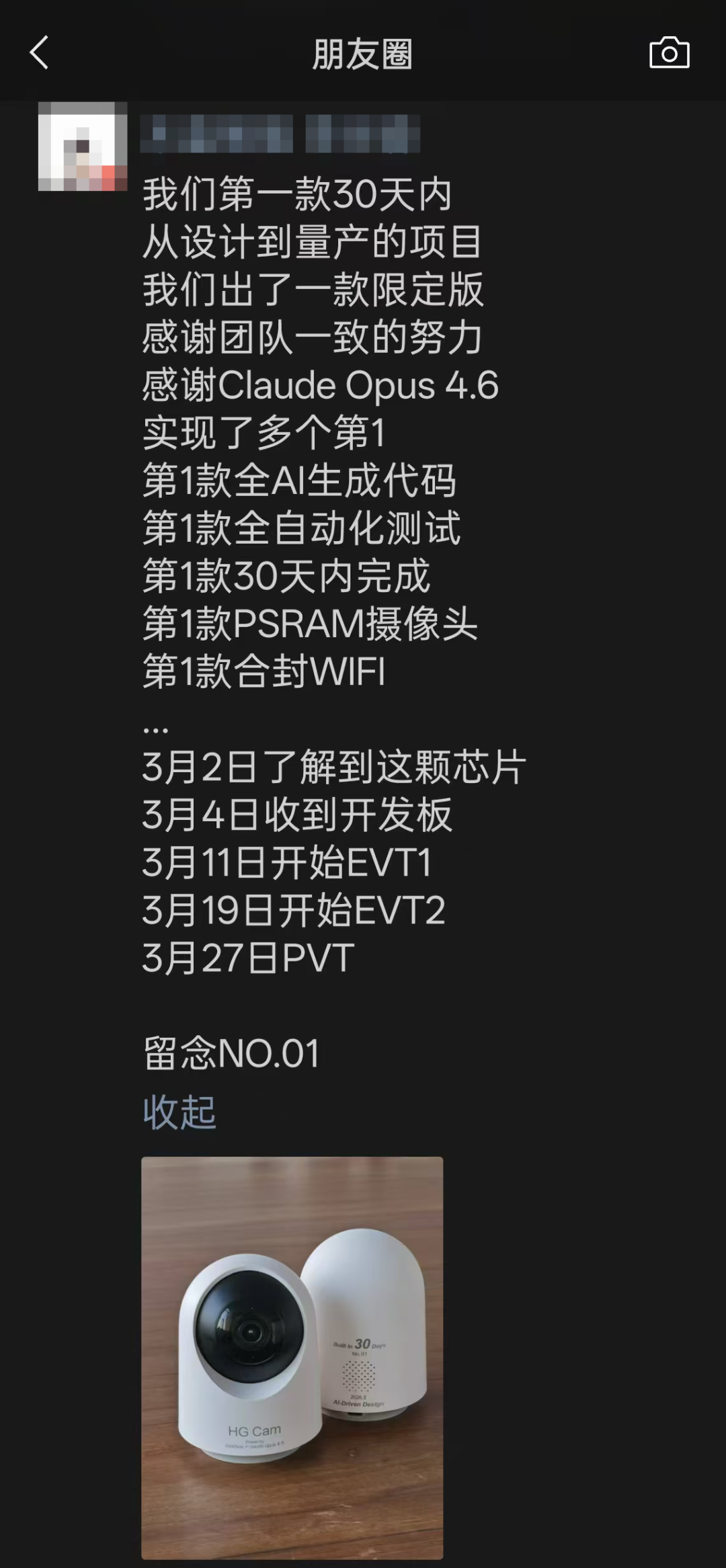
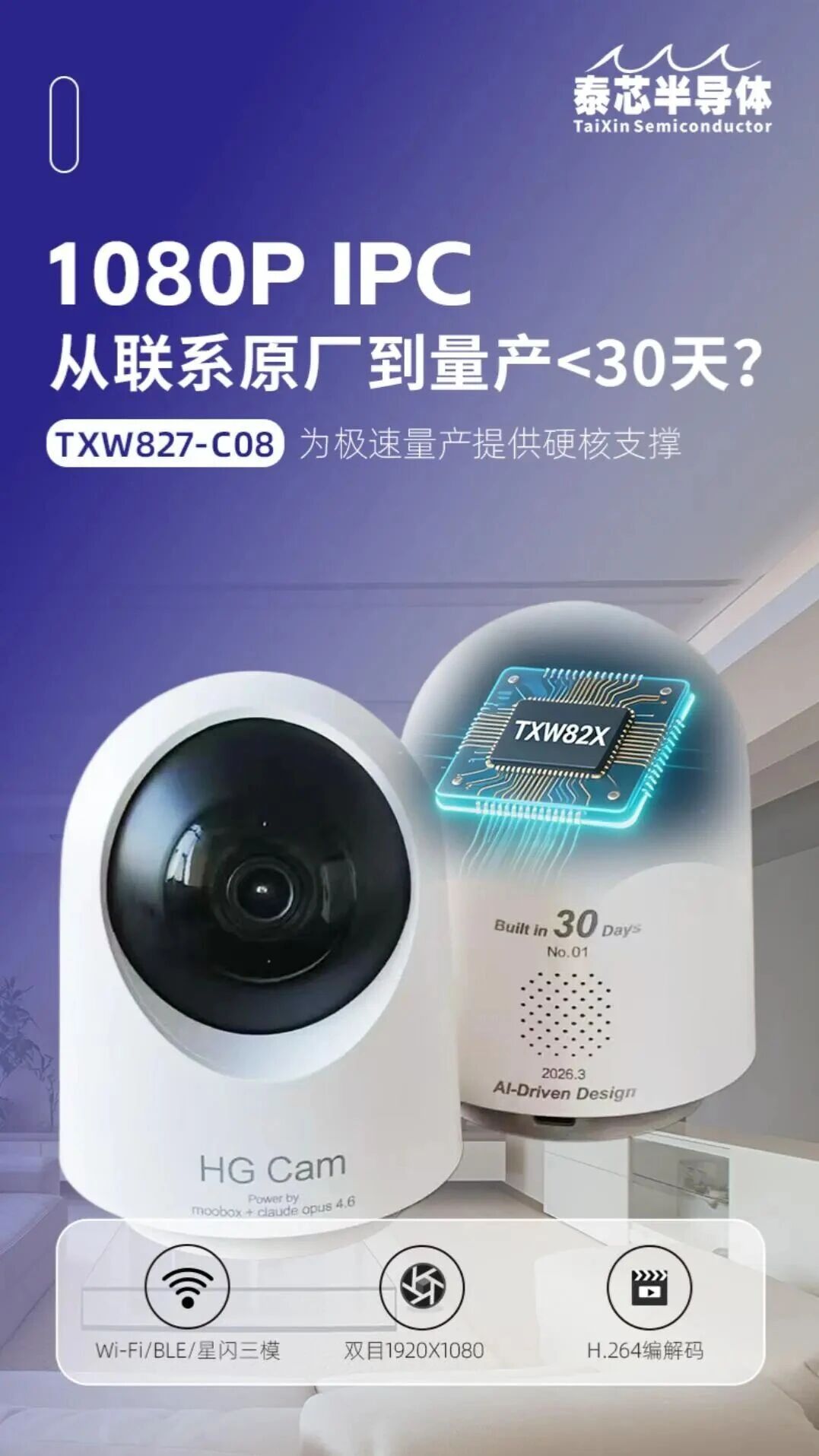
Recently, a limited-edition 1080P smart camera has sparked considerable discussion within the industry. Printed on the product enclosure are"AI-Driven Design"and"Power by Claude Opus 4.6"two lines of text—behind these annotations lies a new hardware development philosophy that is being implemented:Grounded in a domestic high-integration SoC chip, with AI large models participating throughout the code generation process, from contacting Taixin Semiconductor to mass production took less than a month, and the first batch of products has already been shipped to the US.
Traditionally, moving a smart hardware device from solution confirmation to mass production delivery often takes 3 to 6 months. Code development, hardware adaptation, and testing verification require back-and-forth iteration at every stage. Once the cycle drags on, even the best ideas risk missing the market window.
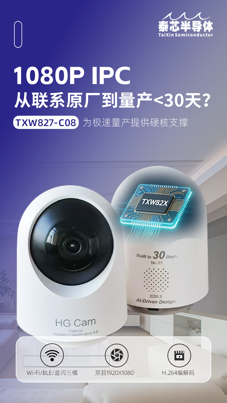
These 30 days have refreshed the speed of development and delivery in the IPC industry

This limited-edition camera features full-code generation participation by the Claude Opus 4.6 large model, supported by a fully automated testing system, achieving multiple breakthroughs in development mode:

Smart Camera with Fully AI-Generated Code:From underlying drivers to application logic, everything is generated with full participation from AI large models, significantly improving development efficiency and code quality
Coverage of Fully Automated Testing System:Multi-dimensional verification of functionality, performance, and stability is completed driven by AI, significantly shortening the testing cycle
30-Day Rapid Mass Production Delivery:Contacted the manufacturer on March 2nd, development board arrived on March 4th, EVT1 validation on March 11th, EVT2 optimization on March 19th, PVT mass production validation on March 27th. The entire closed-loop process took less than 30 days
AI solves the efficiency problem, but what truly makes this possible is the underlying support provided by the chip. Without a main control chip with sufficient performance and perfect adaptation, even the strongest AI R&D efficiency would remain theoretical.
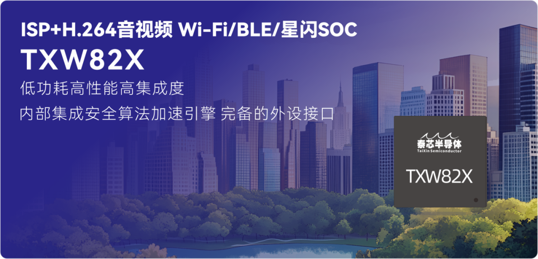
The reason this product achieved such strong product capabilities while completing mass production in just 30 days lies inTXW827-C08 ISP+Audio/Video+Wi-Fi/BLE/SparkLink SOCpowerful enablement.
First, look at the specifications: 2.4GHz Wi-Fi, BLE, and SparkLink triple-mode wireless, dual-core XuanTie E804 processor (up to 240MHz), ISP image processing unit, H.264 hardware encoding/decoding, 8MB PSRAM, Audio ADC/DAC, security encryption engine—all integrated into a single chip. No need for external components, making hardware design naturally faster.
Single-chip integration of the Wi-Fi SOC simplifies peripheral circuits, resulting in a smaller board, lower power consumption, while maintaining smooth transmission of HD images over wireless connections.
In terms of imaging capabilities, the chip features a built-in professional ISP supporting 3A algorithms, 2D/3D noise reduction, and image enhancement. Paired with H.264+MJPEG dual hardware encoding/decoding, it stably outputs 1080P@30fps. It supports MIPI/DVP dual-camera interfaces, covering both monocular and binocular IPC applications.
In terms of computing power, the dual-core E804 supports DSP and floating-point operations. Combined with 368KB SRAM and 8MB PSRAM, it easily handles functions like AI code generation, automated testing, and intelligent video analysis.
Additionally, the SDK development package and reference designs are comprehensive, allowing teams to get started quickly with short debugging cycles. Operating temperature range is -40°C to 85°C, supporting AES/SHA/TRNG encryption, with QFN68 standard packaging—guaranteeing mass production stability.
For development teams, the value of the chip extends far beyond hardware performance itself—comprehensive development toolchains, efficient technical support systems, and deep adaptability with mainstream AI tools allow teams to focus on leveraging AI innovation advantages without worrying about chip adaptation challenges during rapid R&D. Facts prove that the birth of a good product is always a synergistic collaboration between "AI Efficiency" and "Chip Strength".

These 30 days are not an isolated case.
Rather, it is a powerful proof of the replicability of the "AI + Domestic Chips" collaborative innovation model. AI serves as the "accelerator" for efficiency enhancement, while chips act as the "ballast stone" for industrial growth.
This logic extends to broader industry scenarios:
Smart Wearable Devices:Low-power chips accommodate AI-driven rapid feature iterations, shortening new product R&D cycles.
Industrial IoT:High-stability chips support the construction of AI-based automated testing systems, significantly reducing product verification cycles.
Smart Home:Highly integrated chips simplify hardware design, enabling rapid deployment of whole-home smart products when paired with AI tools.
Smart Toys:Highly integrated chips, combined with AI voice interaction and visual recognition capabilities, help toy manufacturers rapidly launch new products with interactive experiences.
Regardless of the scenario, whenever core requirements such as wireless connectivity, smart control, and low-power operation are involved, this "AI Efficiency + Chip Capability" dual-drive model remains applicable, serving as an innovative benchmark for the industry.
From the rapid launch of a limited-edition smart camera to mass innovation breakthroughs across countless industries, the AI era has not diminished the core status of chips; rather, it has further highlighted the value of "premium chips". AI accelerates the R&D process, while chips ensure product quality—both are indispensable. 30 days is not merely a speed record, but a signal of the times: the era of ultra-rapid innovation driven by chip-AI integration has arrived.
This is precisely what Taixin Semiconductor is doing—A chip design enterprise focused on the AIoT domain, possessing technologies such as Wi-Fi, Bluetooth, NearLink, audio/video processing, and edge AI SoCs, continuously driving the adoption of highly integrated SoCs across countless industries.30 days is not the endpoint, but a new starting point for domestic AIoT chips to accelerate empowering innovation across various industries.