

Taixin Semiconductor
Back to products

Wi-Fi SOC Chip

TXW816

Main-model details, variants, and resources

Product Overview

    The TXW816 is a low-power, high-performance, highly integrated 2.4GHz Wi-Fi + Small Wireless multi-mode IoT SOC chip, integrating IEEE 802.11 b/g/n baseband and RF (Radio Frequency) circuits, including Power Amplifier (PA), Low Noise Amplifier (LNA), RF balun, antenna switch, and Power Management Module, among others. 

    The TXW816 Wi-Fi baseband implements Orthogonal Frequency Division Multiplexing (OFDM) technology and is backward compatible with Direct Sequence Spread Spectrum (DSSS) and Complementary Code Keying (CCK) technologies. It supports IEEE 802.11 b/g/n protocols. It supports 20MHz standard bandwidth and 5MHz/10MHz narrow bandwidth, providing a maximum physical layer rate of 72.2Mbit/s. 

    The TXW816 chip integrates a high-performance 32-bit microprocessor, with built-in MJPEG (supporting VGA/720P). It provides rich peripheral interfaces such as DVP, USB2.0 High Speed Device, SDMMC Host, SDIO2.0 Slave, RMII MAC, SPI Master & Device, UART, IIC, IIS, PDM, IR Send/Receive, PWM, GPIO, and ADC/DAC. It supports running programs on SPI Flash. It supports RTOS and third-party components, and comes with an open, easy-to-use development and debugging environment. 

    The TXW816 series includes multiple models, offering the mainstream QFN48 package type. Depending on the package type, the peripheral resource configuration within the device varies. Some packages support built-in PSRAM and Flash. 
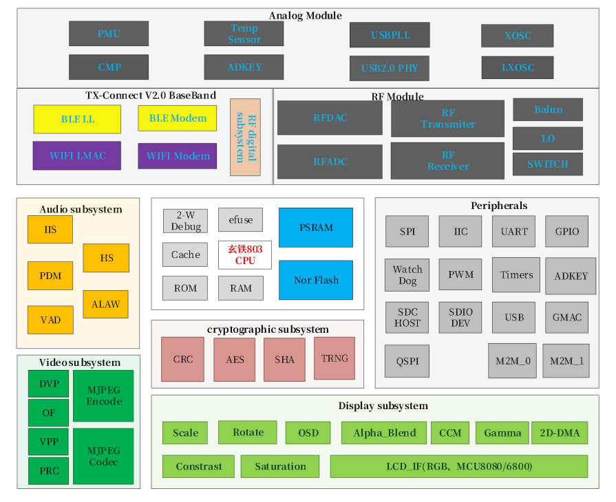
TXW816 architecture diagram

Product Features

Highly Integrated Wi-Fi + BLE Multimode IoT SoC

TXW816 is a low-power, high-performance, highly integrated 2.4GHz Wi-Fi + short-range wireless multimode IoT SoC. It integrates 802.11 b/g/n baseband, RF circuitry, PA, LNA, RF Balun, antenna switch, and power management blocks for wireless audio/video, visual otoscope, aerial imaging, endoscope, and similar products.

Complete Wi-Fi Performance, Up To 72.2Mbps

The chip supports IEEE 802.11 b/g/n with a 1T1R architecture, 20MHz standard bandwidth, and 5MHz/10MHz narrow bandwidth modes. PHY rate reaches up to 72.2Mbps, with STA, AP, AP+STA relay, STA+STA, frame aggregation, RX STBC, and WPA/WPA2/WPA3 security support.

Built-In Video Processing For Audio/Video Products

TXW816 integrates an MJPEG video encoder and MJPEG codec. Video sources can come from DVP, UVC, or SPI camera inputs, supporting up to 1920×1080@30fps, 1280×720@60fps, and 640×480@120fps, plus timestamp, color frame, motion detection, and optical-flow hardware acceleration.

LCD Display And Image Post-Processing

The chip integrates LCD display interfaces and video post-processing modules. It supports RGB, MCU8080, and MCU6800 display interfaces, plus scaling, 90/180/270-degree rotation, horizontal/vertical mirroring, OSD, Alpha Blending, CCM, Gamma correction, saturation adjustment, and contrast adjustment for display-equipped products.

Rich MCU And Peripheral Resources

TXW816 uses a CK803 32-bit CPU up to 240MHz, with 272KB SRAM, SPI Flash/PSRAM expansion, and XIP support. Peripheral resources include up to 34 GPIOs, USB2.0 HS Device, SDIO2.0, SD Host, RMII MAC, QSPI, SPI, IIC, UART, IIS/PCM, PDM, PWM, IR transceiver, ADC/DAC, and more.

Low Power, Security, And Package Options

The chip supports LP/ULP low-power modes with ULP current around 28uA and multiple IO wake-up sources. It integrates AES-128/192/256, SHA256, CRC, SPI Flash firmware encryption, and TRNG. It uses a QFN48 5×5 package, works from -40°C to 85°C, with TXW816-810 including 1MB Flash and TXW816-G00 provided without Flash & PSRAM.

Parameters

ChipChip ModelControllerFrequencyPackageGPIORAM/ROMFlashInterfacesVoltage
T
TXW816
TXW816-G00CK803240QFN4834272*10240PWM, RTC, UART, SPI, IIC, USB3 ~ 3.6
T
TXW816
TXW816-810CK803240QFN4834272*10241024PWM, RTC, UART, SPI, IIC, USB3 ~ 3.6